

Exploring Growth in the Hybrid Bonding Technology Market: Trends, Insights, and Future Outlook
Exploring Growth in the Hybrid Bonding Technology Market: Trends, Insights, and Future Outlook
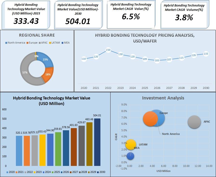
The Hybrid Bonding Technology market is rapidly becoming a cornerstone of advanced semiconductor manufacturing, enabling breakthroughs in performance, size reduction, and power efficiency. As industries seek to create more compact and powerful electronic systems, hybrid bonding provides a critical solution. In 2023, the market stood at USD 333.43 million and is projected to climb to USD 504.01 million by 2030, supported by a healthy CAGR of 6.5% between 2024 and 2030.
Why Hybrid Bonding is Gaining Ground
Hybrid bonding allows for precise and dense interconnects at the wafer and die level, helping manufacturers achieve high-speed communication between stacked chips. This is especially important for applications like AI chips, 5G modules, and high-bandwidth memory systems. With the continuous push for miniaturization and performance, hybrid bonding stands out as the next evolution in chip packaging, delivering superior electrical and thermal performance.
Projecting the Hybrid Bonding Technology Market Size
As companies scale their advanced packaging capabilities, the Hybrid Bonding Technology Market Size is expected to expand significantly. The adoption of this technology is no longer limited to a few high-end applications—it's now being considered across various consumer and industrial electronics segments. Key regions such as Asia-Pacific, especially Taiwan and South Korea, are leading this expansion due to robust investments and an established semiconductor supply chain.
Meanwhile, the U.S. and Europe are ramping up initiatives to bolster local semiconductor manufacturing. This increased global competition and investment are fueling the upward trend in the Hybrid Bonding Technology Market Size, pointing toward long-term sustainable growth.
What the Latest Hybrid Bonding Technology Report Reveals
According to the newest Hybrid Bonding Technology report, several factors are converging to drive this market forward. These include the need for higher I/O density, reduced interconnect latency, and enhanced chip stacking capabilities. The report also outlines some of the challenges in adoption, such as high initial setup costs and the complexity of aligning chips with extreme precision.
Nevertheless, technological advancements—particularly in alignment tools, cleanroom bonding environments, and metrology—are making hybrid bonding more accessible. As process standards improve and equipment becomes more widely available, the barriers to adoption are steadily decreasing.
Final Thoughts: What Lies Ahead for the Hybrid Bonding Technology Market
With hybrid bonding poised to reshape semiconductor architecture, the Hybrid Bonding Technology market offers immense promise for manufacturers, designers, and investors alike. Continuous improvements in material science, packaging techniques, and automation are setting the stage for rapid adoption across mainstream applications. Staying informed on Hybrid Bonding Technology Market Size projections and diving into detailed Hybrid Bonding Technology reports will be essential for stakeholders looking to seize emerging opportunities in this dynamic space.
Information:
Company Name: Mark & Spark Solutions
Contact Person: Sushil W
Email: sales@marksparksolutions.com
Phone: +1-585-374-1088
Website: https://marksparksolutions.com